
When a new device comes out, especially a smartphone, we often read that the built-in processor has a number x di nanometers. But what does this mean? Several users, for obvious reasons, pay little attention to this aspect but we must know that the number of nanometers is quite important if we are looking for a smartphone (or any other device) with a good autonomy. We explain why.
We often talk about x nanometer lithographic process, but what does it mean? Here is what nanometers are on a processor of a device
One of the main technical specifications of a processor is the number of nanometers in its process di manufacture. Over time, this number has further reduced as production progresses. For example, on a top-of-the-range smartphone, it has come to have a lithographic process a 4 nanometers, soon even at 3 nanometers. However, the importance of this unit of measurement is not always clear to users.
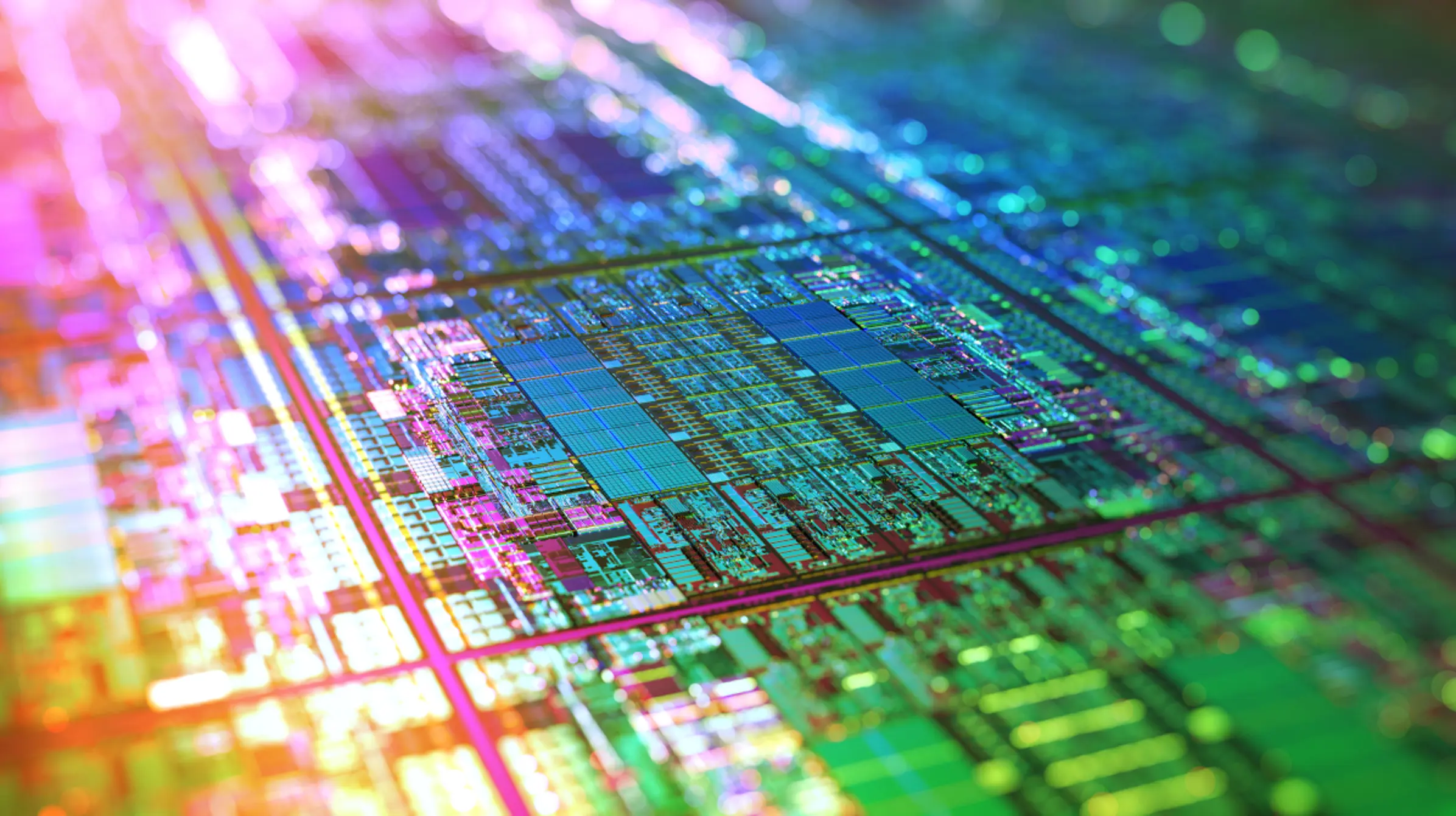
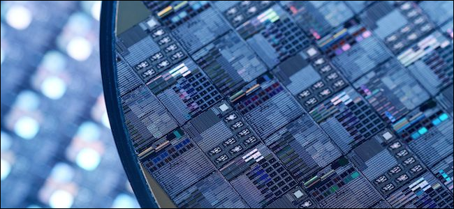
The nanometer (nm) is a unit of measurement of length. To get an idea of the size, 1 nm equals 0,000000001 meter. An infinitesimal measure that is impossible to see with the naked eye. In the specific case of processors, the nanometer refers to the size of transistors that make up the hardware. There are billions of transistors within a specific CPU. Their main function is that of perform calculations using electrical signals.
Read also: Samsung beats TSMC? Development for 3nm chips is underway
By observing this manufacturing process on a mobile phone or computer chip, we can see that unlike other specifications the number decreases with technological advances. Basically, the more the technology goes on, the fewer nanometers between transistors. So why does this happen? There are several benefits that smaller lithography brings to devices. One of the main ones is in the greater efficiency energy. A smaller transistor indicates that less energy is needed for its operation. When considering the complete set of all these micro-components, less use leads to greater autonomy.
As a result of lower consumption, the components end up in generate less heat. In other words, the appliance and machine do not heat up easily and require less cooling during operation. Smaller transistors are also faster and offer higher performance. This is because a low number of nanometers means a smaller distance between them. That is, the electrical signal can be conducted faster. Also, the density is higher, which causes more transistors to fit on the same processor.
In the current technology scenario, depending on the segment or semiconductor developer, we will find mobile processors and platforms with different manufacturing processes. In particular in the smartphone segment (as we said in the introduction) the industry has reached the process to 4 nm (see TSMC and Samsung). This means that the high-end chipsets of the moment such as the A16 Bionic, Snapdragon 8+ Gen 1, Dimensity 9000 Plus and Exynos 2200 work right on this lithograph.
On PCs, AMD's latest Ryzen 7000 family runs on the 5nm node. In turn, Intel still follows its process called “Intel 7”, which uses 10nm fabrication. The next step for the semiconductor industry will be to realize the 3 nm lithography. There is still no precise date on when the devices will arrive, but mass commercial production is expected in 2023.
Read also: Snapdragon 8 Gen 2: the first details of the Qualcomm SoC emerge
TSMC is expected to delay this transition, so the trend is for Samsung to move ahead before it. The Korean company wants to forge ahead and has a program for which it is expected to launch the process a 2 nm by 2025. In addition to this, a node a 1.4 nanometers is expected for 2027. In May 2021, IBM unveiled the world's first chip with 2nm technology. The company's statement at the time detailed the benefits of this knot, such as quadruple the battery life of smartphones, reduce the carbon footprint of data centers, accelerate laptop functions and collaborate for faster object detection in autonomous vehicles.
And will it be possible to get to 1 nm? In October 2016, a study by researchers from the Berkeley Lab showed the creation of a transistor with this node, which promised to break the barrier of the laws of physics. The feat was made possible by replacing silicon with MoS 2 (molybdenum disulfide).